BE Semiconductor (BESI): The Quiet Dutch Company Powering the AI Chip Boom

Everyone knows Nvidia and ASML. Almost nobody talks about the Dutch company sitting on one of the most important bottlenecks in the entire AI supply chain.
When people list the winners of the artificial intelligence boom, the same names come up over and over. Nvidia designs the chips. ASML builds the machines that print them. TSMC manufactures them. But there is a step between manufacturing a chip and putting it inside a data center that has quietly become one of the hardest problems in the industry, and one small company from Duiven in the Netherlands has become the leader in solving it.
That company is BE Semiconductor Industries, better known as Besi. It trades on Euronext Amsterdam under the ticker BESI. And while it is hardly a secret to professional investors anymore, it remains far less known to the wider public than its giant Dutch neighbor ASML. For anyone trying to understand where the value in AI hardware is shifting, Besi is worth a close look.
What Besi actually does
Most of the attention in chipmaking goes to the front end, the part where transistors are etched onto silicon wafers. That is ASML's world. Besi lives in the back end, the part that comes after the wafer is finished. This is the world of assembly and packaging, where individual chips are connected, stacked, and wrapped into something that can actually be installed in a server, a phone, or a car.
Besi designs and builds the machines that do this work. The company operates through three divisions. Die Attach machines place and bond chips onto a surface. Packaging systems mold, trim, and finish the final product. Plating systems apply metal layers and coatings. It sells these tools under brand names that are well known inside the industry, including Fico, Meco, Datacon, and Esec. Its customers are the large chipmakers, the foundries, and the assembly subcontractors that serve them.
For most of its history this was a solid but cyclical business. What changed everything was a technology called hybrid bonding.
Why packaging suddenly matters
For decades the chip industry improved performance by making transistors smaller. That approach, often summarized as Moore's Law, is now slowing down because shrinking transistors further has become extraordinarily expensive and physically difficult.
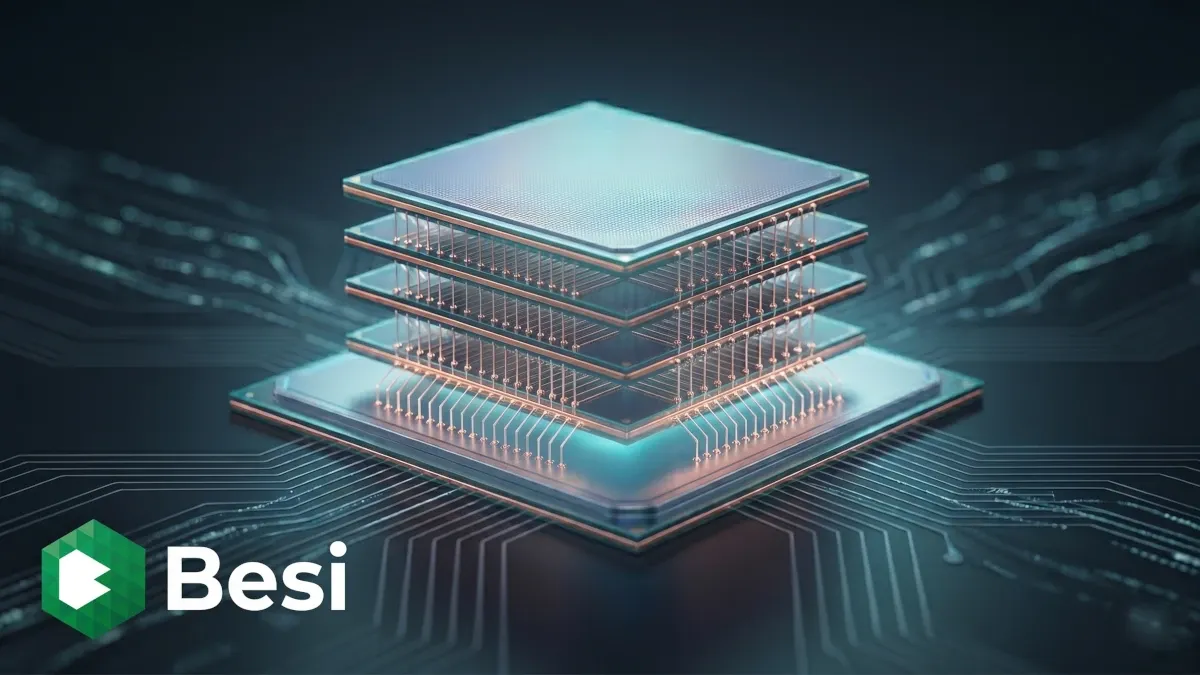
So the industry found a different path. Instead of only making each chip smaller, engineers now stack multiple chips together and connect them as tightly as possible. This is called advanced packaging. The idea is that if you cannot make a single chip much faster, you can combine several specialized chips, called chiplets, and stack memory directly on top of logic. The package itself becomes part of the performance story rather than just a protective shell.
This matters enormously for AI. Modern AI accelerators rely on stacks of high bandwidth memory, known as HBM, sitting right next to powerful logic dies. The faster and tighter you can connect those pieces, the more performance you get. Packaging capacity has become one of the real bottlenecks limiting how quickly AI chips can be produced.
Hybrid bonding, explained simply
Traditionally, chips were stacked using tiny balls of solder called bumps. Picture two circuit boards connected by hundreds of microscopic solder dots. It works, but the bumps take up space, they limit how densely you can pack connections, and they create heat and reliability problems as you push them closer together.
Hybrid bonding removes the bumps entirely. Instead of solder dots, the copper pads on two chips are polished until they are almost perfectly smooth and then fused directly together, copper to copper. The result is a connection that is far denser, faster, more power efficient, and more reliable. To pull this off you need machines that can align two chips with accuracy below ten nanometers, which is a fraction of the size of a virus. This is extremely difficult, and Besi is the leader at doing it.
This is the heart of the investment case. Besi is not selling a commodity tool. It is selling one of the most precise machines in the world for a process that the entire AI industry increasingly depends on.
Who needs this technology
The list of companies moving toward hybrid bonding and advanced packaging reads like a who is who of the chip world. TSMC uses its SoIC platform for 3D stacking. Intel has its Foveros Direct approach. AMD has built chiplet based products such as the MI300 line for AI. Memory makers are moving toward hybrid bonding for future HBM generations. And a newer application, co packaged optics, which brings fiber optic connections directly onto the chip package, is opening up yet another growth avenue.
Besi sits in the middle of this shift, and it does not stand alone. Applied Materials, one of the largest equipment makers in the world, became Besi's largest shareholder with a roughly nine percent stake and has been a long term partner on hybrid bonding development. Analysts at Bank of America have gone so far as to describe Besi as potentially the ASML of hybrid bonding, pointing to the dominant market share they expect it to hold as the technology scales.
The numbers tell the story
The financial results show the shift is real and accelerating. In 2025 Besi reported revenue of around 591 million euros. In the first quarter of 2026 the momentum picked up sharply. Revenue rose more than 28 percent compared with a year earlier, net income jumped almost 64 percent, and orders more than doubled, growing over 104 percent year over year. The gross margin came in around 63.5 percent, a level most industrial companies can only dream of.
The most striking signal came on June 18 2026, when Besi held its investor day. Management raised its long term financial targets, lifting the revenue goal from a range of 1.5 to 1.9 billion euros up to a range of 1.7 to 2.2 billion euros. It also raised the lower end of its operating margin target from 40 to 45 percent, keeping the top end at 55 percent. The reason given by chief executive Richard Blickman was a clear improvement in demand for AI data center applications, photonics, and new uses of hybrid bonding across logic, memory, and co packaged optics.
Put simply, a company that did under 600 million euros of revenue last year is now telling investors it sees a path toward two billion or more, at operating margins that would rank among the best in the entire technology sector.
What the analysts are saying
Sentiment among professional analysts has turned strongly positive, and several major banks raised their price targets in the days around the investor day. The table below shows the most recent targets, all carrying a buy rating.
| Date (2026) | Institution | Rating | Price target |
|---|---|---|---|
| June 22 | Bank of America | Buy | 401 euros |
| June 22 | ABN AMRO Oddo | Buy | 400 euros |
| June 19 | UBS | Buy | 370 euros |
| June 16 | Redburn | Buy | 350 euros |
Across the broader analyst panel the picture was six buy ratings, zero hold, and two sell, with an average target around 326 euros.
The reasoning behind the most bullish calls is worth understanding. Bank of America analyst Didier Scemama argues that Besi is the best positioned company to benefit from 3D stacking and chiplet architecture, in both logic and memory. After the investor day he raised his 2028 revenue estimate to 1.95 billion euros and his earnings per share estimate to 10.69 euros, figures that sit roughly 19 and 25 percent above the broader consensus. He even suggested his own estimates might still be too cautious, noting that Besi itself is guiding toward selling far more hybrid bonding machines than most analysts currently model.
UBS struck a similar tone, calling Besi a rare asset for investors who want exposure to the structural growth in advanced packaging, while acknowledging openly that the shares are already richly valued.
The risks worth knowing
A fair analysis has to include the other side, and there are real risks.
The first is valuation. Besi has already risen more than 100 percent in 2026 and trades at a very high earnings multiple. A great company and a great stock are not always the same thing, and much of the optimism is already priced in. Notably, the average analyst target sits below where the most bullish banks are, which tells you the market has run hard.
The second is cyclicality. The chip equipment industry has always moved in waves of boom and bust. Besi has been hit before by sudden order cancellations, and a downturn in the broader semiconductor cycle would not spare it.
The third is concentration and geopolitics. A large share of revenue comes from Asia, including significant exposure to China, which makes the company sensitive to export restrictions and trade tensions that are an ongoing theme in the chip world.
Finally, the dividend has historically been variable rather than steady, because the company prefers to keep flexibility to invest. Investors looking for reliable income should keep that in mind.
The bottom line
Besi is a rare combination. It is small enough to still fly under the radar of many everyday investors, yet it holds a leading position in a technology that the largest names in AI increasingly cannot do without. It has high margins, a strong balance sheet, accelerating orders, and a backer in Applied Materials that signals how strategically important its technology has become.
The valuation is demanding and the cycle is real, so this is not a risk free story. But for anyone trying to understand where the next layer of value in AI hardware is being created, the answer is no longer only about who designs the fastest chip. Increasingly it is about who can connect those chips together. On that question, a quiet company from Duiven is one of the most important names in the world.
This article is for general information and education. It is not investment advice or a recommendation to buy or sell any security. Always do your own research before investing.